Last updated 10/2024
MP4 | Video: h264, 1920×1080 | Audio: AAC, 44.1 KHz
Language: English | Size: 404.31 MB | Duration: 0h 56m
Part 6: Advanced Semiconductor Materials and Technologies
What you’ll learn
Gain insights into the factors that limit or enable semiconductor device improvements
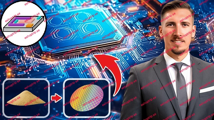
Learn about cutting edge technologies like EUV lithography, TAIKO, DBG, SD, Advanced Packaging (2.5D, 3D, Interposer, HBM, TSV, UBM, RDL) and more
Understand the interdependencies between different technologies
Learn about Moore`s law and how this defines semiconductor improvement actions
Requirements
Interest in electronics and semiconductors
Description
Embark on an enlightening journey into the world of semiconductors with our comprehensive 7-part course on Udemy! This meticulously crafted series will equip you with a deep understanding of the semiconductor industry, from its fundamental physics to cutting-edge technologies and business strategiesIn Part 1, we’ll dive into the “Fundamentals of Semiconductor Physics”, unraveling the mysteries of electron behavior, energy bands and the principles that make these miraculous materials work. You’ll gain a solid foundation that will serve as the bedrock for your semiconductor knowledge.Part 2 explores “Semiconductor Business Models”, offering invaluable insights into the industry’s economic landscape. Learn how companies navigate this high-stakes, fast-paced market and position themselves for success.Parts 3 and 4 focus on the critical aspects of semiconductor production. In “Hard Production Necessities”, you’ll discover the intricate processes and equipment required to manufacture these tiny technological marvels. “Auxiliary Production Necessities” will complement this knowledge, covering the supporting systems and infrastructure that enable seamless production.Part 5 delves into the various “Roles2 within the semiconductor industry. Gain an understanding of the diverse career paths available and the skills required to thrive in this dynamic field.In Part 6, we’ll explore “Advanced Semiconductor Materials and Technologies”, keeping you at the forefront of innovation. From novel materials to emerging fabrication techniques, you’ll be well-versed in the future of semiconductor technology.Finally, Part 7 covers “Semiconductor Reliability and Failure Analysis”, a crucial aspect of quality control and product improvement. Learn the techniques used to ensure the longevity and performance of semiconductor devices.By the end of this course, you’ll have a comprehensive understanding of the semiconductor environment, from the atomic level to industry-wide trends. Whether you’re a student, professional or technology enthusiast, this course will provide you with the knowledge and insights to navigate the fascinating world of semiconductors.
Overview
Section 1: Einführung
Lecture 1 Introduction
Lecture 2 Moore`s law
Lecture 3 How to increase semiconductor device performance
Lecture 4 EUV lithography
Lecture 5 TAIKO
Lecture 6 DBG (Dicing before grinding)
Lecture 7 SD (Stealth dicing)
Lecture 8 Advanced semiconductor materials (SiC, GaN)
Lecture 9 Introduction into advanced packaging
Lecture 10 SoC (System on chip)
Lecture 11 SiP (System in package) and flip-chip technology
Lecture 12 Interposer
Lecture 13 2.5D and 3D packaging
Lecture 14 WLP (Wafer level packaging)
Lecture 15 HBM (High bandwidth memory)
Lecture 16 Key takeaways
Newcomers and experts within the semiconductor industry
https://anonymz.com/?https://www.udemy.com/course/the-semiconductor-environment-part-6/
